BSNL J.T.O. Recruitment Exam 2001
Paper-I
1. A second-order system has a transfer function given by ![]() If the system, initially at rest is subjected to a unit step input at t = 0, the second peak in the response will occur at
If the system, initially at rest is subjected to a unit step input at t = 0, the second peak in the response will occur at
(A) π sec
(B) π/3 sec
(C) π/2 sec
(D) 2π/3 sec
2. The open-loop transfer function of a feedback control system is ![]() The gain margin of the system is
The gain margin of the system is
(A) 2
(B) 8
(C) 4
(D) 16
3. A silicon sample is uniformly doped with 1016 phosphrous atoms/cm3 and 2 × 10¹⁶ boron atoms/cm3. If all the dopants are full ionized, the material is
(A) p-type with carrier concentration of 2 × 10¹⁶/cm3
(B) p-type with carrier concentration of 1016/cm3
(C) n-type with carrier concentration of 1016/cm3
(D) T2-will get damaged and T1 will be safe.
4. The initial contents of the 4-bit serial-in-parallel-out, right-shift, Shift Register shown in fig. is 0110. After 3 clock pulses are applied, the contents of the Shift Register will be

(A) 1 1 1 1
(B) 0 1 0 1
(C) 1 0 1 0
(D) 0 0 0 0
5. shows the circuit of a gate in the Resistor Transistor Logic (RTL) family. The circuit represents a
(A) NAND
(B) OR
(C) NOR
(D) AND
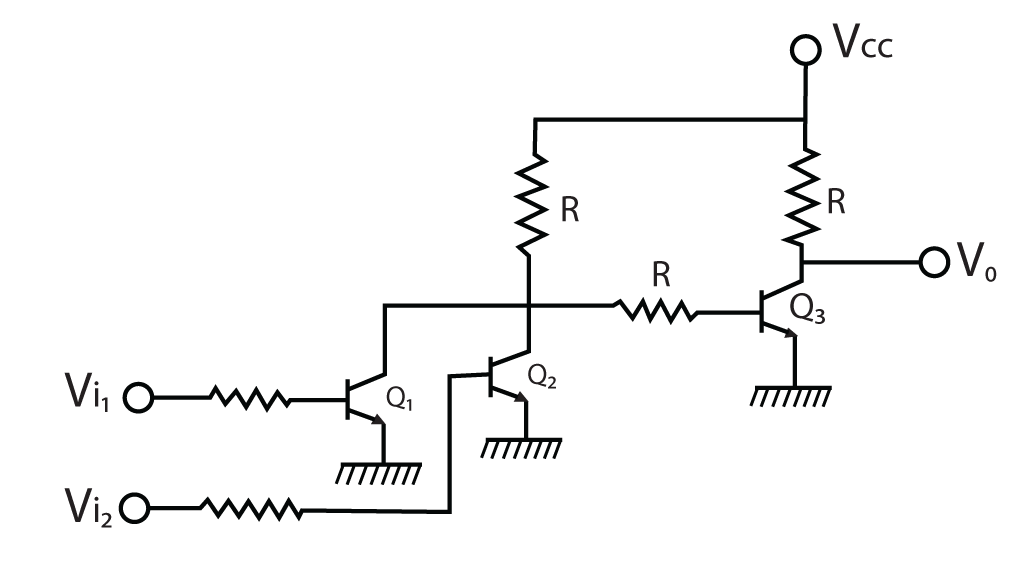
6. The logic realized by the circuit shown in Fig. is
(A) F = B . C
(B) F = A ⊕ C
(C) F = A . C
(D) F = B + C
7. In a multicavity magnetron, strapping is employed primarily
(A) to prevent mode jumping
(B) to increase the output of the magnetron
(C) to reduce the back heating of the cathode
(D) to increase the separation between the resonant frequencies in the π-mode and in the adjacent modes
8. A Lissajous pattern, as shown in Fig. is observed on the screen of a CRO when voltages of frequencies fx and fy are applied to the x and y plates respectively. fx : fy is then equal to

(A) 3 : 2
(B) 1 : 2
(C) 2 : 1
(D) 2 : 3
9. In the transistor circuit shown in Fig. collector-to-ground voltage is +20 V. Which of the following is the probable cause of error?
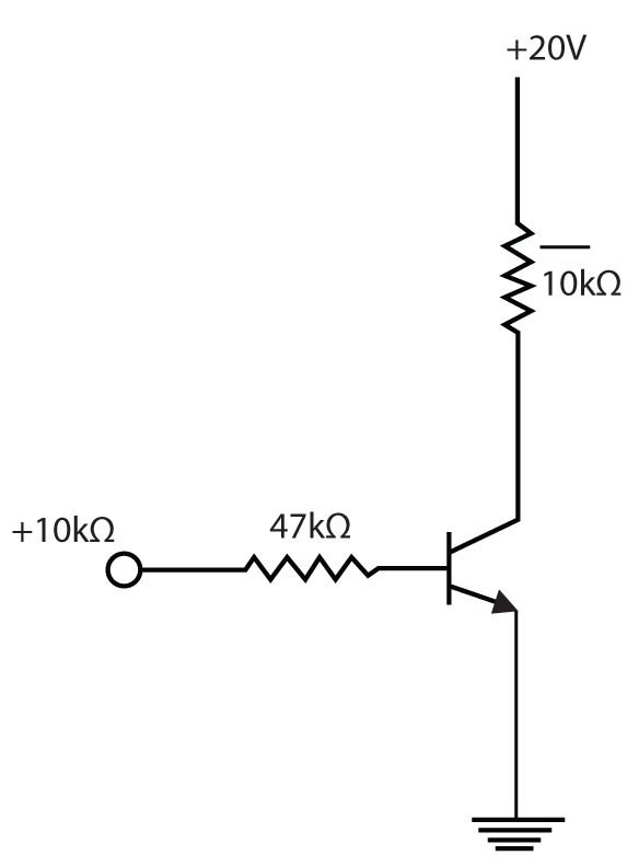
(A) Emitter to ground connection open
(B) Collector-emitter terminals shorted
(C) 10kΩ resistor open
(D) Collector-base terminals shorted
10. Part of the digital phase meter is shown in the fig. If the input signals are VB(t) = VR sin ωt and VP(t) = VP sin(ωt + 30°) the reading of the meter will be
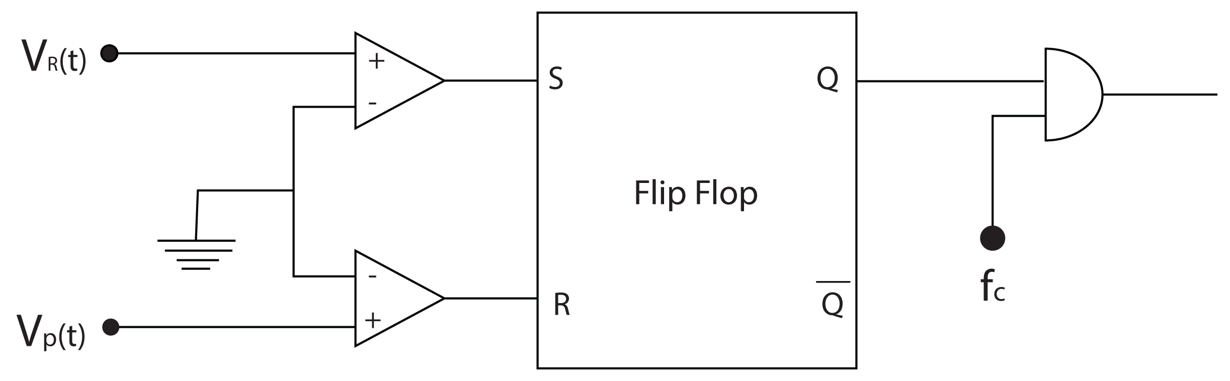
(A) 210°
(B) 330°
(C) 150°
(D) 30°
11. The response of an initially relaxed linear constant parameter network to a unit impulse applied at t = 0 is 4 e−2tu(t). The response at this network to a unit step Function will be:
(A) (1 – 4e−4t)u(t)
(B) 4[e−t – e−2t] u(t)
(C) sin 2t
(D) 2[1 – e−2tu(t)]
12. The open circuit impedance matrix of the 2-port network shown in Fig. is
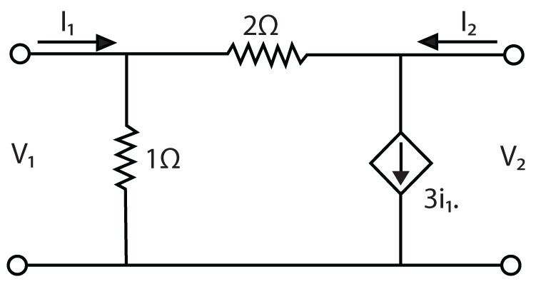
(A) 
(B) 
(C) 
(D) 
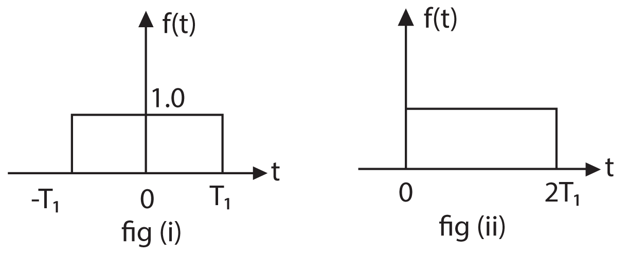
13. The impulse response and the excitation function of a linear time invariant causal system are shown in Fig. (i) and (ii) respectively. The output of the system at t = 2 sec is equal to
 .
.
(A) 0
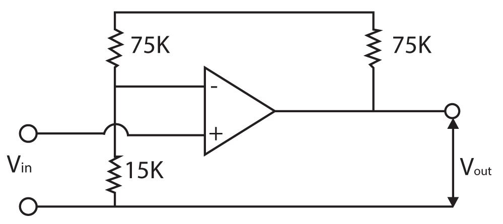
(B) 3/2
(C) 1/2
(D) 2
14. An electromechanical closed-loop control system has the following characteristic equation
s3 + 6Ks2 + (K + 2) s + 8 = 0
where K is the forward gain of the system.
The condition for closed loop stability is
(A) K = −0.528
(B) K = 2
(C) K = 0
(D) K = 0.528
15. In a uniformaly doped abrupt p-n junction, the doping level of the n-side is four time the doping level of the p-side. The ratio of the depletion layer width is
(A) 2.0
(B) 0.5
(C) 1.0
(D) 0.25
16. LEDs have response time of the order of
(A) 100 ns
(B) 1 ns
(C) 0.1 ns
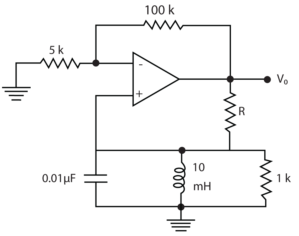
(D) 1 μs
17. Zero mean white noise is passed through an ideal low pass filter with cut off at W Hz. The filter output will be uncorrelated at time instants spaced
(A) ![]()
(B) ![]()
(C) ![]()
(D) 
18. A 4HGz carrier is DSBSC modulated by low pass message signal with maximum frequency of 2 MHz. The resultant signal is to be ideally sampled. The minimum frequency of the sampling in train should be
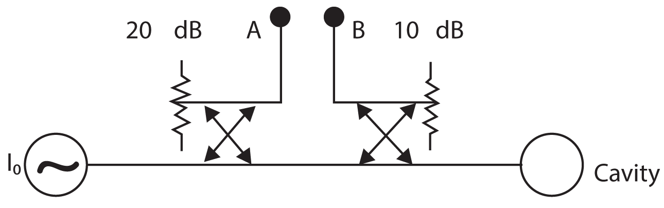
(A) 4 MHz
(B) 8 MHz
(C) 8.004 GHz
(D) 8 GHz
19. Which of the following field equations indicate that the free magnetic changes do not exist
(A) ![]()
(B) ∇ ∙ H = 0
(C) ![]()
(D) ∇ × H = J
20. Two isotropic antennas are separated by a distance of two wavelengths. If both the antennas are fed with currents of equal phase and magnitude, the number of lobes in the radiation pattern in the horizontal plane are
(A) 6
(B) 4
(C) 2
(D) 8
21. Value of R in the oscillator circuit shown in Fig. is so chosen that is just oscillates at an angular frequency of ω. The value of ω and the required value of R will respectively be
(A) 2 × 10⁴ rad/sec, 2 × 10⁴Ω
(B) 105 rad/sec’ 2 × 10⁴Ω
(C) 2 × 10⁴ rad/sec, 105Ω
(D) 105 rad/sec, 105Ω
22. The following sequence of instruction are executed by an 8085 microprocessor
1000 LXI SP, 27 FF
1003 CALL 1006
1006 POP H
The contents of the stack pointer (SP) and the HL, register pair on completion of execution of these instructions are
(A) SP = 27 FF, HL = 1006
(B) SP = 27 FD, HL = 1003
(C) SP = 27 FF, HL = 1003
(D) SP = 27 FD, HL = 1006
23. A 1 km long microwave link uses two antennas each having 30 dB gain. If the power transmitted by one antenna is a 1 W at 3 GHz, the power received by the other antenna is approximately
(A) 98.6 μW
(B) 76.8 μW
(C) 55.2 μW
(D) 63.4 μW
24. A rectangular air-filled waveguide has cross section of 4 cm × 10 cm. The minimum frequency which can propagate in the waveguide is
(A) 1.5 GHz
(B) 3.0 GHz
(C) 2.5 GHz
(D) 2.0 GHz
25. A deterministic signal has the power spectrum given in Fig. The minimum sampling needed to completely represent this signal is
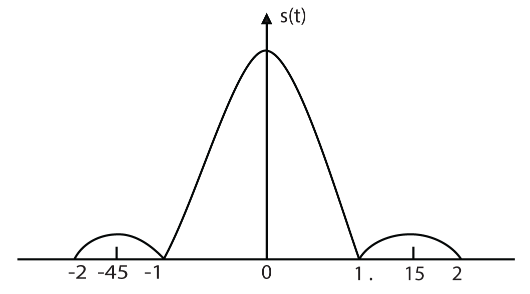
(A) 3 kHz
(B) 2 kHz
(C) 1 kHz
(D) None of the above
26. The decoding circuit show in fig. has been used to generate the active low chip select signal for microprocessor peripheral. (The address lines are designated as A2 to A7 for I-O address)

The peripheral will correspond to IO address in the range
(A) 60 H to 63 H
(B) 30 H to 33 H
(C) A 4 H to A 7 H
(D) 70 H to 73 H
27. In a J – K flip-flop we have J = 1, K = 1. Assuming the flip flop was initially cleared and then clocked for 6 pulses, the sequence at the Q output will we

(A) 010101
(B) 011001
(C) 010010
(D) 010000
28. In the MOSFET amplifier of fig, the signal outputs V1 and V2 obey the relationship
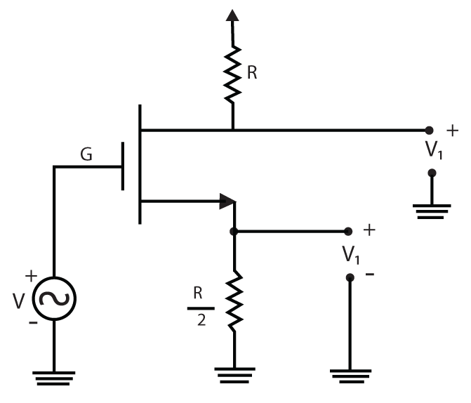
(A) V1 = V2/2
(B) V1 = −2V2
(C) V1 = 2V2
(D) V1 = −V2/2
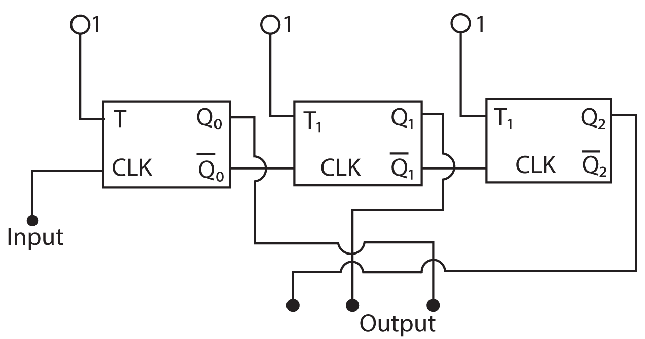
29. shows a mod-K counter. Here K is equal to

(A) 1
(B) 4
(C) 3
(D) 2
30. The time averaged Poynting vector in W/m2, for a wave with ![]() in free space is
in free space is
(A) ![]()
(B) ![]()
(C) ![]()
(D) ![]()
31. In the circuit, C0 is the distributed capacitance of the coil and C is the tuning capacitor. If C = C1 for the fundamental harmonic frequency and C = C2 for the second harmonic frequency, then the value of C0 can be expressed as
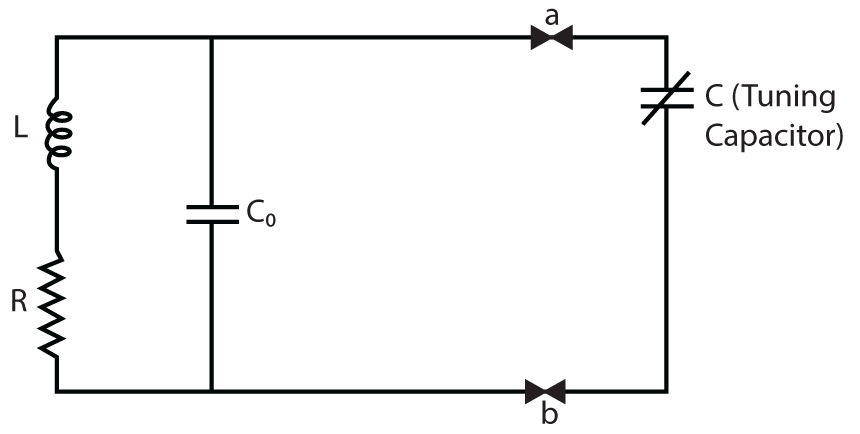
(A) ![]()
(B) ![]()
(C) ![]()
(D) ![]()
32. The 3dB bandwidth of a typical second-rode system with the transfer function  is given by
(A) ![]()
(B) ![]()
(C) ![]()
(D) ![]()
33. A small concentration of minority carries is injected into a homogeneous semiconductor crystal at one point. An electric field of 10 V/cm is applied across the crystal and this moves the minority carriers a distance of 1 cm is 20 μ The mobility (in cm2/volt.sec)
(A) 5,000
(B) 2,000
(C) 1,000
(D) 500,000
34. v(t) = 5[cos(106πt) – sin(103πt) x sin (106πt)] represents
(A) AM signal
(B) DSB suppressed carrier signal
(C) SSB upper sideband signal
(D) Narrow band FM signal
35. The drift velocity of electros, in silicon
(A) is proportional to the electric field for all values of electric field
(B) is independent of the electric field
(C) increase linearly with electric field at low values of electric field and gradually saturates at higher values of electric field
(D) increases at low values of electric field and decreases at high values of electric field exhibiting negative differential resistance
36. The diffusion potential across a P-N junction
(A) does not depend on doping concentrations
(B) increases with decreasing band gap
(C) decreases with increasing doping concentration
(D) increases with increase in doping concentrations
37. The output of the circuit show in Fig. is equal to

(A) 1
(B) 0
(C) ![]()
(D) ![]()
38. A 12-bit ADC is operating with a 1μ sec clock period and the total conversion time is seen to be 14μ The ADC must be of the
(A) flash type
(B) integrating type
(C) counter type
(D) successive approximation type
39. A uniform plane wave in air is normally incident on an infinitely thick slab. If the refractive index of the glass slab is 1.5 then the percentage of the incident power that is reflected from the air-glass interface is
(A) 100%
(B) 4%
(C) 20%
(D) 0%
40. A silicon a MOSFET has a threshold voltage of 1 V and oxide thickness of 400 A°. [εr (SiO2) = 3.9, ε0 = 8.854 × 10⁻¹⁴ F/cm, q = 1.6 × 10⁻¹⁰ C]. The region under the gate is ion implanted for threshold voltage tailoring. The dose and type of the implant (assumed to be a sheet charge at the interface) required to shift the threshold voltage to −1Vare
(A) 1.08 × 10¹²/cm2, p – type
(B) 1.08 × 10¹²/cm2, n – type
(C) 5.4 × 10¹¹/cm2, n – type
(D) 5.4 × 10¹¹/cm2, p – type
41. For a flip-flop formed from two NAND gates as shown in fig. The unusable state corresponds to

(A) X = 0, Y = 0
(B) X = 0 , Y = 1
(C) X = 1, Y = 0
(D) X = 1, Y = 1
42. Fig. shows the electrostatic vertical deflection system of CRT. Given that VA is the accelerating voltage, the deflection sensitivity (deflection/volt) is proportional to
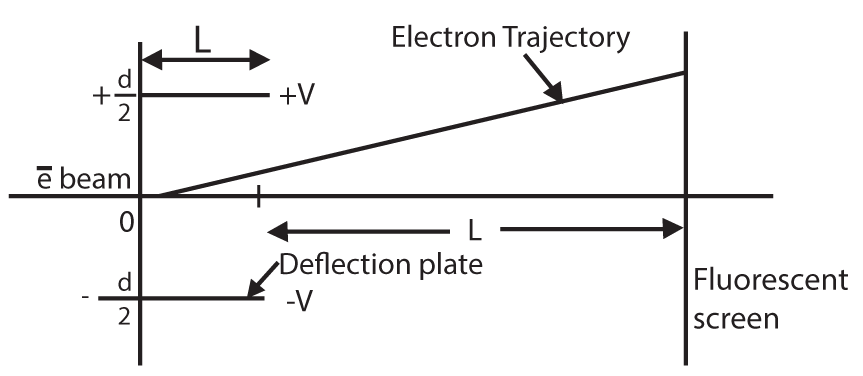
(A) ![]()
(B) ![]()
(C) ![]()
(D) ![]()
43. Fig. shows the input attenuator of a multimeter. The meter reads full scale with 12V at M, with the range switch at position ‘q’. What is the required voltage at M to obtain full scale deflection with the range switch at position ‘s’?
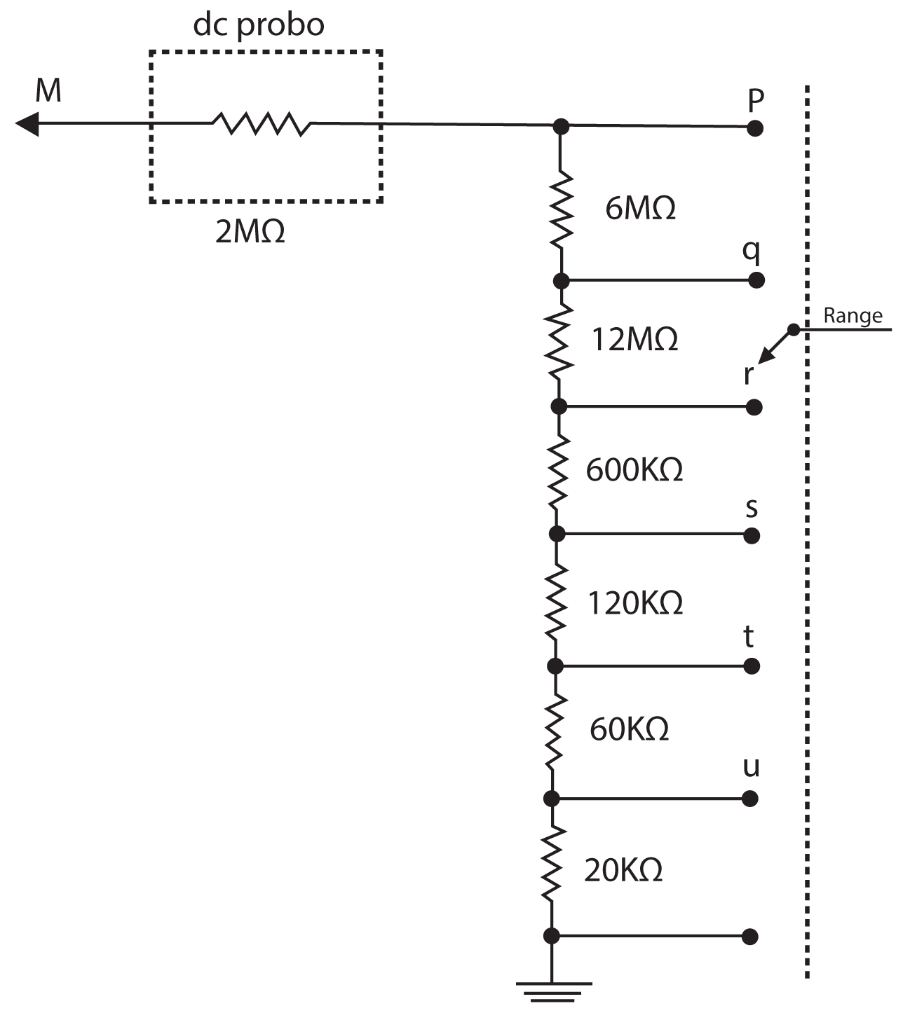
(A) 1 V
(B) 120 V
(C) 150 V
(D) 147 V
44. Viewed from the terminals A, B the following circuit shown in fig. can be reduced to an equivalent circuit of a single voltage source in series with a single resistor with the following parameters
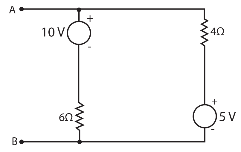
(A) 5 volt source in series with 10Ω resistor
(B) 1 volt source in series with 2.4Ω resistor
(C) 1 volt source in series with 10Ω resistor
(D) 15 volt source in series with 2.4 Ω resistor
45. The phase lead compensation is used to
(A) increase rise time and decrease overshoot
(B) decrease rise time and increase overshoot
(C) increase both rise tie and overshoot
(D) decrease both rise time and overshoot
46. Gauss-Seidal iterative method can be used for solving a set of
(A) linear algebraic equations only
(B) linear differential equations only
(C) both linear and non-linear algebraic equations
(D) both linear and nonlinear differential equations
47. For the system shown in fig. with a damping ratio ζ of 0.7 and an undamped natural frequency ωn of 4 rad/sec, the values of K an a are
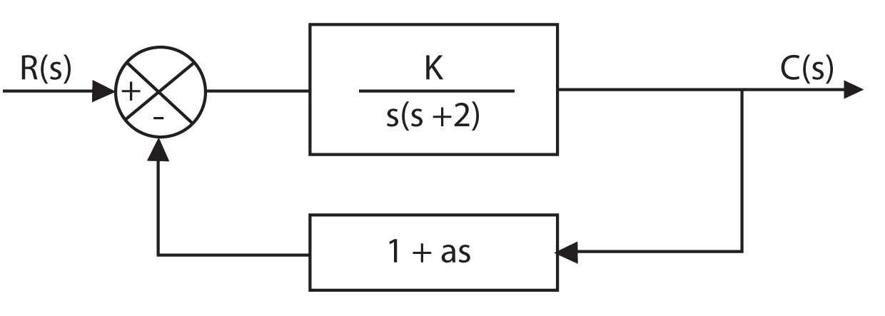
(A) K = 4, a = 0.35
(B) K = 64, a = 0.9
(C) K = 16, a = 0.225
(D) K = 8, a = 0.455
48. A water boiler at home is switched on to the a.c. mains supplying power at 230 V/50 Hz. The frequency of instantaneous power consume by the boiler is
(A) 0 Hz
(B) 150 Hz
(C) 100 Hz
(D) 50 Hz
49. In the circuit shown in fig. X is an element which always absorbs power. During a particular operations, it sets up a current of 1 amp in the direction shown and absorbs a power Px. It is possible that X can absorb the same power Px for another current i, the value of this current is
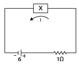
(A) ![]()
(B) ![]()
(C) 5 amps
(D) none of these
50. Two concentric square loops A and B carry equal currents in the same direction. The magnetic field at O due to the two loops A and B will be in the ratio
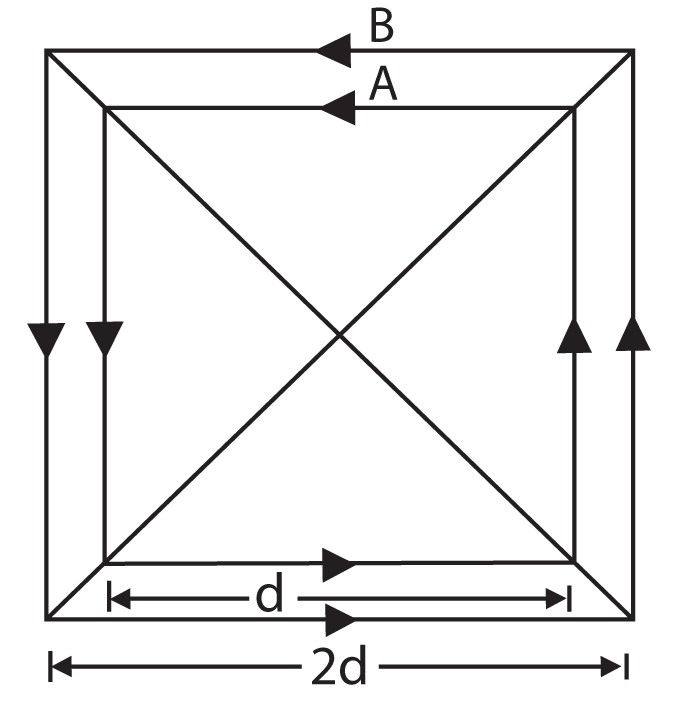
(A) 1 : 1.414
(B) 2 : 1
(C) 1.414 : 1
(D) 1 : 1
PAPER-II
51. The amplitude modulated waveform s(t) = Ac[1 + Kam(t)] cos ωct is fed to an ideal envelope detector. The maximum magnitude of Kam(t) is greater than 1. Which of the following could be the detector output?
(A) Acm(t)
(B) Ac[1 + Kam(t)]2
(C) |Ac[1 + Kam(t)]
(D) ![]()
52. An 8 bit successive approximation analog to digital converter has a full scale reading of 2.55 V and its onversion time for an analog input of 1V is 20
(A) 40 μs
(B) 20 μs
(C) 10 μs
(D) 50 μs
53. Maximum phase-lead of the compensator ![]() is
is
(A) 55 degrees at 12 rad/sec
(B) 52 degrees at 10 rad/sec
(C) 52 degrees at 4 rad/sec
(D) None of these
54. The characteristic equation of a feedback control system is 2s4 + s3 + 3s2 + 5s + 10 = 0. The number of roots in th right half of s-plane are
(A) 0
(B) 3
(C) 2
(D) 1
55. A step down chopper operate from a dc voltage source Vs and feeds a dc motor armature with a back emf Eb. From oscilloscope traces, it is found that the current increases for time t, falls to zero over time tf and remins zero for time to in every chopping cycle. Then the average dc voltage across the freewheeling diode is
(A) 
(B) 
(C) 
(D) 
56. A dual-slope analog-to-digital converter uses an N-bit counter. When the input signal Va is being integratd, the counter is allowed to count up to a value
(A) equal to 2N – 1
(B) equal to 2N – 2
(C) proportional to Va
(D) inversely proportional to Va
57. A current of [2 + √2 sin(314t + 30°) + 2√2 cos (952t + 45°)] is measured with a thermocouple type, 5 A full-scale, class 1 meter. The meter reading would lie in the range.
(A) 5A ± 1%
(B) 2A ± 2.5%
(C) 3A ± 1.7%
(D) (2 + 3√2) A ± 1%
58. The voltage phasor of a circuit is V and the current phasor is The active and the reactive powers in the circuit are
(A) 10 W and 1732 VAR
(B) 5 W and 8.66 VAR
(C) 20√2 W and 10√2 VAR
(D) 20 W and 60 VAR
59. A fixed capacitor of reactance –j0-02Ω is connected in parallel across a series combination of a fixed inductor of reactance j0.01Ω and a variable resistance R. As R is varied from zero infinity, the diagonal of the admittance of this L-C-R circuit will be
(A) a semi-circle of diameter j 50 and center at zero
(B) a semi-circle of diameter j 100 and center at zero
(C) a straight line inclined at an angle
(D) a straight line parallel to the x-axis
60. The function corresponding to the Bode plot of fig. is
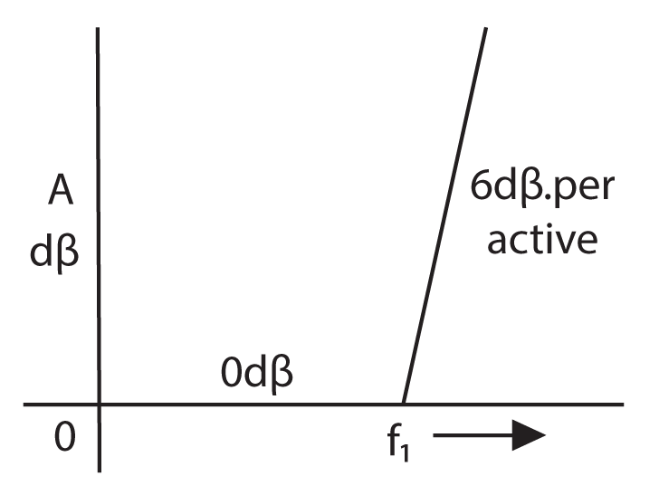
(A) A = j f/f1
(B) A =1/(1 – j f1/f)
(C) A = 1/(1 + J f1/f)
(D) A = 1 + j f/f1
61. A parabolic dish has a diameter of 10 m. The maximum possible (ideal) gain of the antenna at λ = 314 cm will be
(A) 50 dB
(B) 40 dB
(C) 30 dB
(D) 60 dB
62. Microwave antenna aperture efficiency depends on
(A) feed pattern
(B) surface losses
(C) antenna aperture
(D) low side lobe level
63. Which one of the following is the Fourier transform of the signal given in Figure (i) if the Fourier transform of the signal in Figure (ii) is given by ![]() ?
?
(A) ![]()
(B) ![]()
(C) ![]()
(D)![]()
64. A conductor having surface density σ is embedded in a dielectric medium of permittivity ε. The electric field in the medium is E. If it is known that the pressure p on the conductor surface is equal to the electric energy density in the medium, then p (in SI units) is given by
(A) ![]()
(B) ![]()
(C) ![]()
(D) ![]()
65. The semiconductor diode which can be used in switching circuits at microwave range is
(A) Gunn diode
(B) varactor diode
(C) tunnel diode
(D) PIN diode
66. Noise temperature (T) and gain (G) are two important parameters of satellite antennas. Which one of the following antennas has the largest G/T ratio?
(A) Parabolic reflector
(B) Pyramidal horn antenna
(C) Cassegranian antenna
(D) Dipole antenna
67. A square waveguide carries TE11 mode whose axial magnetic field is given by ![]() where the waveguide dimensions are in centimeters. What is the cut-off frequency of the mode?
where the waveguide dimensions are in centimeters. What is the cut-off frequency of the mode?
(A) 6.5 GHz
(B) 7.5 GHz
(C) 5 GHz
(D) 8 GHz
68. Under what condition will the instrumentation amplifier circuit given in the figure possess highest CMRR? (Rs1 and Rs2 source resistances)
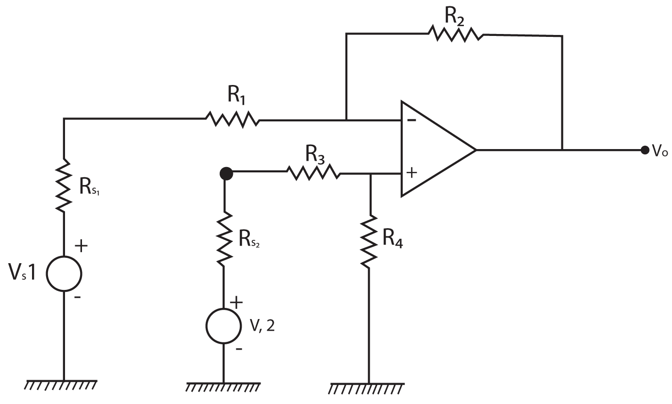
(A) ![]()
(B) ![]()
(C) ![]()
(D) ![]()
69. In the root-locus for open-loop transfer function ![]() the break away and break in points are located respectively at
the break away and break in points are located respectively at
(A) −7.73 and +4.27
(B) −2.47 and −3.77
(C) −4.27 and −7.73
(D) −2 and −1
70. An amplifier operating over the frequency range o f 18 to 20 MHz has a 10k Ω input resistance. The RMS noise voltage at the input to the amplifier at ambient temperature of 27℃ is (Assume the Boltzman constant value as 1.38 × 10⁻²³ J/K)
(A) 16.2 microvolts
(B) 17.2 microvolts
(C) 18.2 microvolts
(D) 14.2 microvolts
71. An infinite number of concentric rings carry a charge Q each alternately positive and negative. Their radii are 1, 2, 4, 8 .. meters in geometric progression as shown. The potential at the centre of the will be
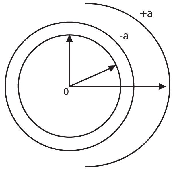
(A) ![]()
(B) ![]()
(C) ![]()
(D) ![]()
72. If the vector ![]() represents a magnetic field, then the value of k must be
represents a magnetic field, then the value of k must be
(A) −1
(B) 2
(C) 1
(D) −2
73. Two isotropic antennas are separated by a distance of two wavelengths. If both the antennas are with currents of equal phase and magnitude, the number of lobes in the radiation pattern in the horizontal plane is
(A) 2
(B) 6
(C) 4
(D) 8
74. In a rectangular cavity resonator having a = width, b = height and d = length for a > b < d. the dominant mode is
(A) TE101
(B) TM110
(C) TE110
(D) TM101
75. The arrangement shown in figure represents an RC potentiomer for measuring ac voltage. What should be the value of C so that V0/Vin is independent of the frequency of the input signal?
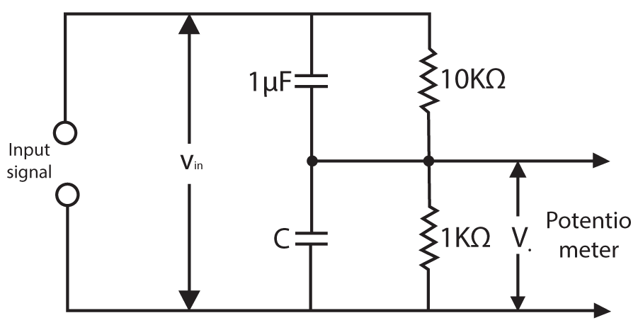
(A) 0.10 μF
(B) 11 μF
(C) 10 μF
(D) 0.09 μF
76. The Q factor of a radio coil is
(A) independent of frequency
(B) increases monotonically as frequency increases
(C) increases upto a certain frequency and then decreases beyond that frequency
(D) decreases monotonically as frequency increases
77.Which of the following oriented graphs have the same fundamental loop matrix?
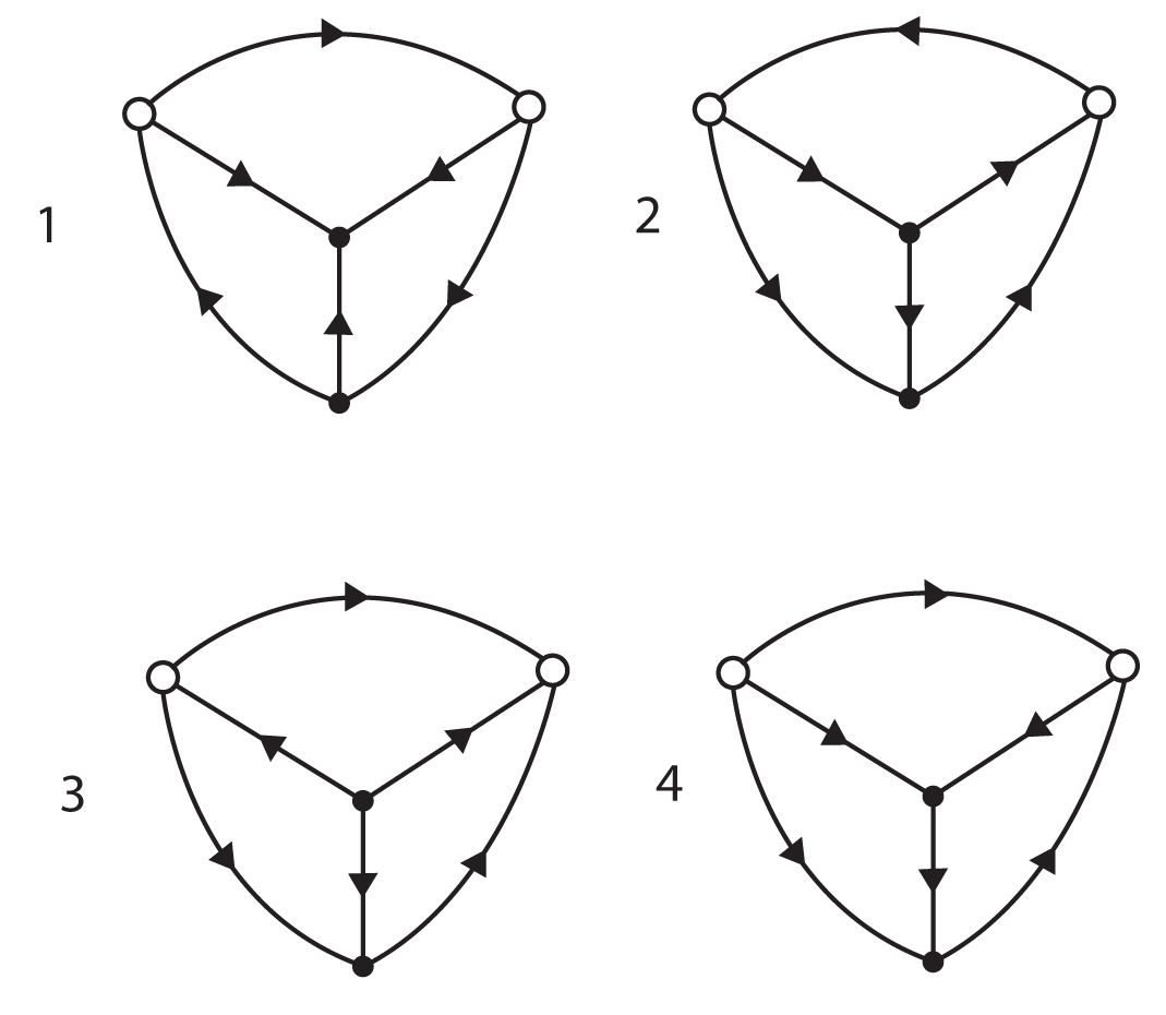
Select the correct answer using the codes given below:
(A) 1 and 2
(B) 1, 3 and 4
(C) 2 and 3
(D) 2, 3 and 4
78. The logic circuit given below converts a binary code y1y2y3 into
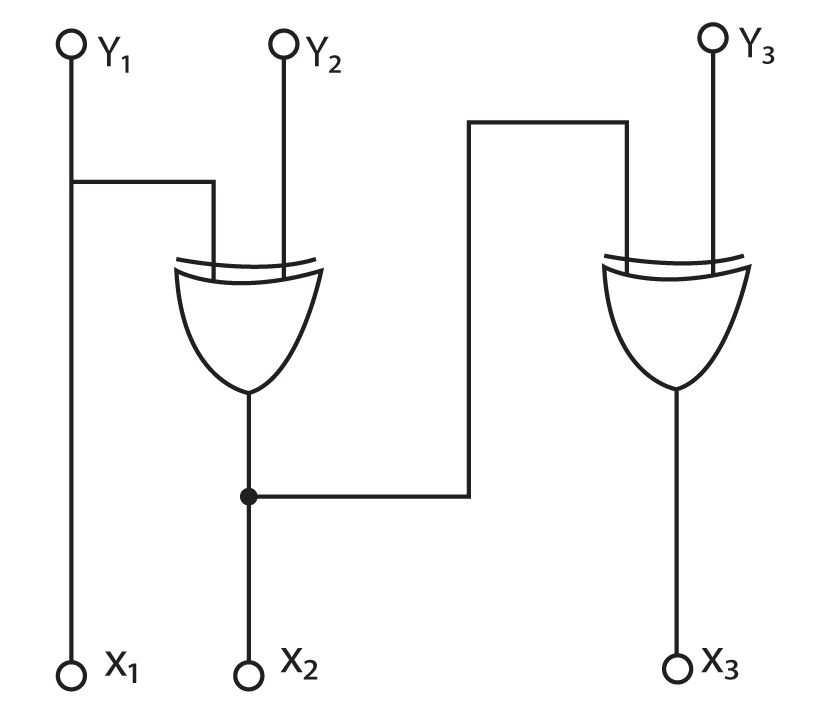
(A) Excess-3 code
(B) BCD code
(C) Gray code
(D) Hamming code
79. A control system is as shown in figure. The maximum value of gain K for which the system is stable is
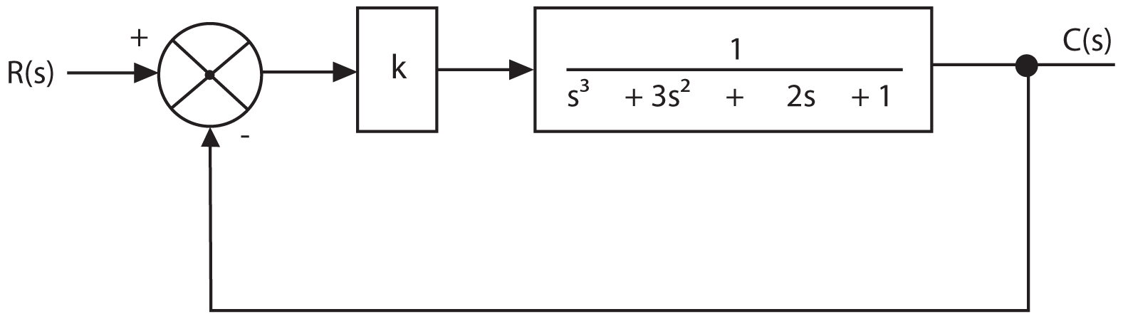
(A) √3
(B) 4
(C) 3
(D) 5
80. The demarcation between Fresnel region and Fraunhofer region fairly approximated by minimum distance between antennas for pattern measurement is (given that R = distance between antennas, D = largest aperture dimension and λ = wavelength)
(A) R = 2 D2/λ2
(B) R = λ2/2 D2
(C) R = 2 D2/ λ
(D) R = λ/2 D2
81. Measurement of Hall Effect coefficient in a semiconductor provides information on the
(A) sign of charge carriers alone
(B) mass and concentration of charge carriers
(C) sign and mass of charge carriers
(D) sign and concentration of charge carriers
82. The circuit shown in figure is a
(A) monostable multivibrator
(B) bootstrap sweep circuit
(C) Miller sweep circuit
(D) frequency division circuit
83. The input pulses to the different stages of the counter shown in figure must be of
(A) constant frequency and constant width
(B) variable frequency but constant width
(C) constant frequency but variable width
(D) variable frequency as well as variable width
84. The capacity of an analog communication channel with 4 kHz bandwidth and 15 dB SNR is approximately
(A) 20,000 bps
(B) 8,000 bps
(C) 10,000 bps
(D) 16,000 bps
85. Which one of t he following is a transferred electron device?
(A) BARITT diode
(B) Gunn diode
(C) IMPATT diode
(D) Step recovery diode
86. The slow-wave structures of a TWT is provided with an attenuator. Which one of the following is the function of such an attenuator?
(A) It prevents the RF power from reaching the output of the device when the beam is switched on
(B) It reduces the noise level of the device
(C) It prevents oscillations in the device
(D) It is used to broadband of the device
87. On a resistively terminated high frequency loss-less transmission line fed by a 500 MHz source, the VSWR is found to be equal to 2 and the first voltage minimum is measured at 30 cm from the load end. What is the value of the “normalized” load resistance?
(A) 3
(B) 2
(C) 1/4
(D) 1/2
88. In the voltage regulator shown in Fig. the load current can vary from 100 mA to 500 mA. Assuming that the Zener diode is ideal (i.e., the Zener knee current is negligibly small and Zener resistance is zero in the breakdown region), the value of R is
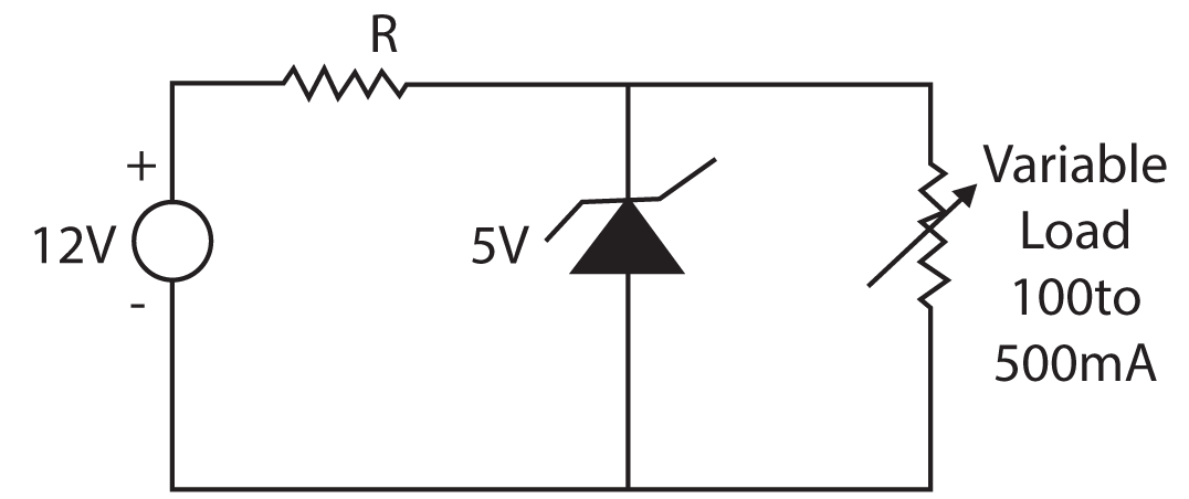
(A) 7Ω
(B) 70Ω
(C) ![]()
(D) 14Ω
89. Assume that the op-amp of fig. is ideal. If vi is a triangular wave, then v0 will be
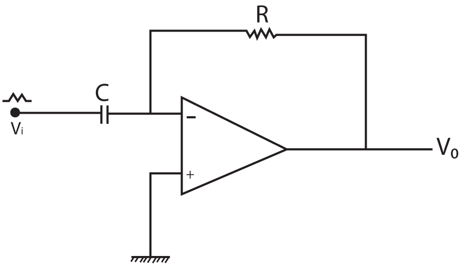
(A) triangular wave
(B) square wave
(C) parabolic wave
(D) sine wave
90. Two carriers 40 MHz and 80 MHz respectively are frequency modulated by a signal of frequency 4 kHz, such that the band-widths of the FM signal in the two cases are the same. The peak value deviation in the two cases are in the ratio of
(A) 1 : 4
(B) 1 : 2
(C) 1 : 1
(D) 2 : 1
91. What is the slope change at ω = 10 of the magnitude v/s frequency characteristic of a unity feedback system with the following open-loop transfer function?
![]()
(A) −40 dB/dec to −20 dB/dec
(B) −20 dB/dec to −40 dB/dec
(C) 40 dB/dec to 20 dB/dec
(D) 40 dB/dec to −20 dB/dec
92. For the circuit shown in the figure, the instantaneous current ii(t) is
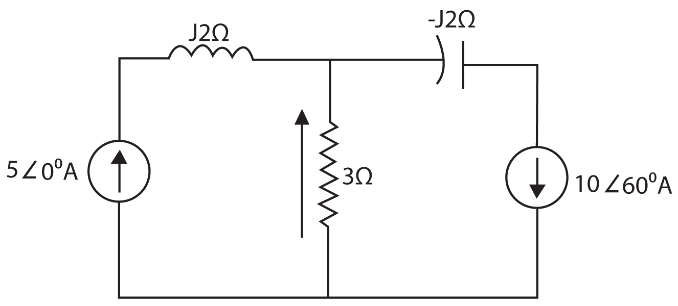
(A) ![]()
(B) ![]()
(C) 5∠60° amps
(D) 5∠−60° amps
94. A JFET is set up as source follower. Given, μ = 200, rd = 100 K and source load resistance RL = 1 K. The output resistance R0 is given approximated by
(A) 1000Ω
(B) 500 Ω
(C) 333 Ω
(D) 666 Ω
95. The given figure shows a reflectometer arrangement to measure the parameters of an over coupled one-port cavity resonator at f0. With 100 mW of input power, the output power at B is 6.4 mW. What is the value of the coupling coefficient represent?
(A) 9
(B) 2.5
(C) 5
(D) 6.4
96. Two coils having equal resistances but different inductances are connected in series. The time constant of the series combination is the
(A) sum of the time constants of the individual coils
(B) average of the time constants of individual coils
(C) geometric mean of the time constants of the individual coils
(D) product of the time constants of the individual coils
97. An antenna of input resistance 73Ω is connected to a 50Ω If losses are ignored, then its efficiency will be nearly
(A) 0.19
(B) 0.81
(C) 1.19
(D) 0.97
98. A uniform plane electromagnetic wave travelling in free-space enters into a lossless medium at normal incidence. In the medium its velocity reduces by 50% and in free-space sets up a standing wave having a reflection coefficient of −125. The permeability of the medium is,
(A) 2.57 μ0
(B) 1.60 μ0
(C) 1.26 μ0
(D) 3.5 μ0
99. In the graph shown in fig. for the tree with branches b, d and f, the fundamental loops would include
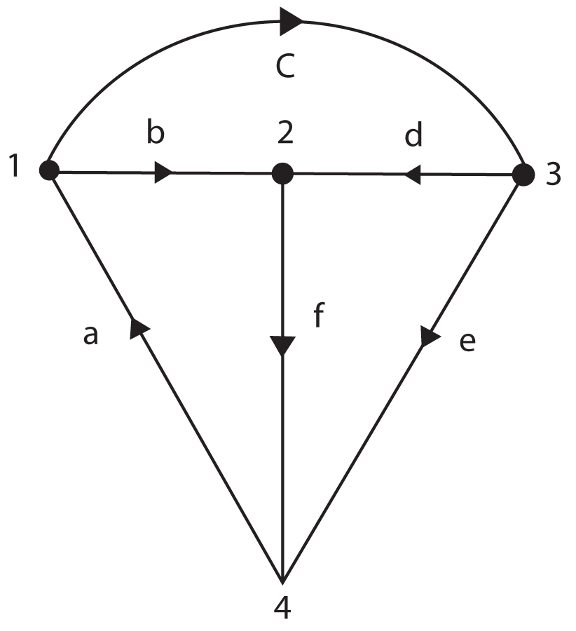
1, 2, 3, 4 are nodes
a, b, c, d, e f are branches
(A) abc, def, bdea
(B) adb, def, bfa
(C) cea, bdea, abc
(D) abde, def, cdb
100. An amplifier without feedback has a gain of 1000. The gain with a negative feedback of 0.009 is
(A) 1000
(B) 10
(C) 100
(D) 125
PAPER-III
101. “Dakshina Gangotri” is
(A) The place from where Ganga originates
(B) first nuclear submarine acquired by India
(C) India’s permanent station at Antartica
(D) A tributary or river Ganges
102. Which one of the following rulers built the Bibi Ka Maqbara?
(A) Akbar
(B) Shahjahan
(C) Jahangir
(D) Aurangzeb
103. Hunter Commission was appointed by the British Government to probe into
(A) Chauri Chaura incident
(B) demolition of Kanpur Mosque
(C) Kakori train dacoity incident
(D) Jalianwalla Bagh tragedy
104. Chilka lake is situated in
(A) Andhra Pradesh
(B) West Bengal
(C) Assam
(D) Orissa
105. India’s fifth Atomic power plant is being constructed is
(A) Narora (U.P.)
(B) Kaiga (Karnataka)
(C) Kakrapar (Gujarat)
(D) Rawa bhata (Rajasthan)
106. What does Angstrom measure?
(A) Intensity of light
(B) speed at flowing water
(C) volume of liquids
(D) Length of light waves
107. The phenomenon of “midnight Sun” is caused by the
(A) inclination of earth’s axis
(B) rotation of the earth on its axis
(C) sun spots
(D) nuclear explosions
108. Which one of the following is associated with the Gupta Age of Indian history?
(A) Visit of Chinese pilgrim Husan Tsang
(B) Significant contribution to poetry and literature by Banabhatta
(C) Significant contribution to Indian astronomy by Aryabhatta
(D) Macedonian invasion
109. Under-12 World Chess Championship in 1998 was won by
(A) Tejas Bakre
(B) Koneru Humpy
(C) Vijayalakshmi
(D) Dibyendu Barua
110. One of the most important foreign exchange earning herbs used in the treatment of several kinds of chronic dysentery is
(A) Isabgol
(B) Tulsi
(C) Madhuca
(D) Rauwolfia
111 to 114 : Direction-Read the passages that follows. The questions at the end of teach passage are based on the content to the passage. Choose your answers from the choice mentioned.
The need for sola electricity is clear. It is safe, ecologically sound, efficient, continuously available, and it has no moving parts. The basic problem with the use of solar photovoltaic devices is economics, but until recently every little progress had been made towards the development of low-cost photovoltaic devices. The larger part of research funas has been devoted to study of single-crystal silicon solar cells, despite the evidence, including that of the leading manufacturing of crystalline silicon, that this technique holds little promise. The reason for this pattern is understandable and historical. Crystalline silicon is the active element in the very successful semi conductor industry and virtually all of the solid state devices contain silicon transistors and diodes. Crystalline silicon, however is particularly unsuitable to terrestrial solar cells.
Crystalline silicon solar cells work well and are successfully used in the space programme, where cost is not an issue. While single crystal silicon has been p proven in extraterrestrial use with efficiencies as high as 18% and other more expensive and scarce materials such as gallium arsenide can have even higher efficiencies, costs must be reduced by a factor of more than 100 to make them practical for commercial uses. Besides the fact that the starting crystalline silicon is expensive, 95% of it is wasted and does not appear in the final device. Recently there have been some imaginative attempts to make polycrystalline and ribbon silicon that are lower in cost than high quality single crystals; but to data the efficiencies of these apparently lower-cost arrays have been unacceptably small. Moreover, these materials are cheaper only because of the introduction of disordering in crystalline semiconductors, and disorder degrades the efficiency of crystalline solar cells.
The dilemma can be avoided by preparing completely disordered or amorphous materials Amorphous materials have disordered atomic structure as compared to crystalline materials, that is, they have only short-range order rather than the long-range periodicity of crystals. The advantage of amorphous solar cells are impressive. Whereas crystals can be grown as wafers about 4 inches in diameter, amorphous materials can be grown over large areas in a single process. Whereas crystalline silicon must be made 200 microns thick to absorb a sufficient amount of sun light for efficient energy conversion, only 1 micron of the proper amorphous materials is necessary. Crystalline silicon solar cells cost in excess of Rs. 100 per square foot, but amorphous films can be created at a cost of about 50 paise per square foot.
Although many scientists were aware of the very low cost of amorphous solar cells, they felt that they could never be manufactured with the efficiencies necessary to contribute significantly to the demand for electric power. This was based on a misconception about the feature which determines efficiency. For example, it is not the conductivity of the material in the dark that is relevant that only the photoconductivity, that is, the conductivity in the presence of sunlight. Already, solar cells with efficiencies will above 6% have been developed using amorphous materials and further research will doubtless find even less costly amorphous materials with higher efficiencies.
111. The material in the passage could best the used in an argument for
(A) discontinuing the space programme
(B) further study of the history of silicon crystals
(C) increased funding for research on amorphous materials
(D) increased reliance on solar energy
112. The author mentions which of the following as advantages of amorphous materials for solar cells over silicon crystals?
I. the relative thinness of amorphous materials
II. the cost of amorphous materials
III. the size of solar cells which can be made of amorphous material
(A) I and II only
(B) II only
(C) I only
(D) II and III only
113. The tone of the passage can best be described as
(A) analytical and optimistic
(B) tentative and inconclusive
(C) critical and discouraged
(D) biased and unprofessional
114. The author is primarily concerned with
(A) explaining the functioning of solar cells
(B) discussing the importance of solar energy
(C) presenting a history of research on energy sources
(D) describing a possible solution to the problem of the cost of photovoltaic cells
Questions (115 to 116): Direction- In this section a number of sentences are given. The sentences are underlined in three separate parts and each one is labeled (a), (b), (c). Read each sentence to find out whether there is an error in any underlined part. No sentence has more than one error. When you find an error in any one of the underlined parts (a), (b) or (c), indicates your response on the separate Answer Sheet at the appropriate space. You may feel that there is no error in a sentence. In that case letter (d) will signify a ‘No error’ response.
115. Perhaps the governments too in its efforts
(a)
to make the truth being know
(b)
should take some sincere steps in that direction
(c)
No error
(d)
116. An open administration will not help
(a)
if government rules are complicated and incomprehensible
(b)
for the affected public
(c)
No error
(d)
117. Find the most similar word in meaning
BRAGGADOCIO
(A) encounter
(B) boasting
(C) weaponry
(D) position
118. Find the most similar word in meaning
INCORRIGIBLE
(A) narrow
(B) unreformable
(C) inconceivable
(D) straight
119. Find the opposite word in meaning
CARNAL
(A) actual
(B) minute
(C) spiritual
(D) impressive
120. Find the opposite word in meaning
JETTISON
(A) salvage
(B) descend
(C) submerge
(D) decelerate
BSNL Junior Telecom Officers’ (JTO) Recruitment Exam Question Paper 2014 With Answer Key
BSNL Junior Telecom Officers’ (JTO) Recruitment Exam Question Paper 2008 With Answer Key
BSNL Junior Telecom Officers’ (JTO) Recruitment Exam Question Paper 2005 With Answer Key
BSNL Junior Telecom Officers’ (JTO) Recruitment Exam Question Paper 2002 With Answer Key
BSNL Junior Telecom Officers’ (JTO) Recruitment Exam Question Paper 2001 With Answer Key
Latest Govt Job & Exam Updates: